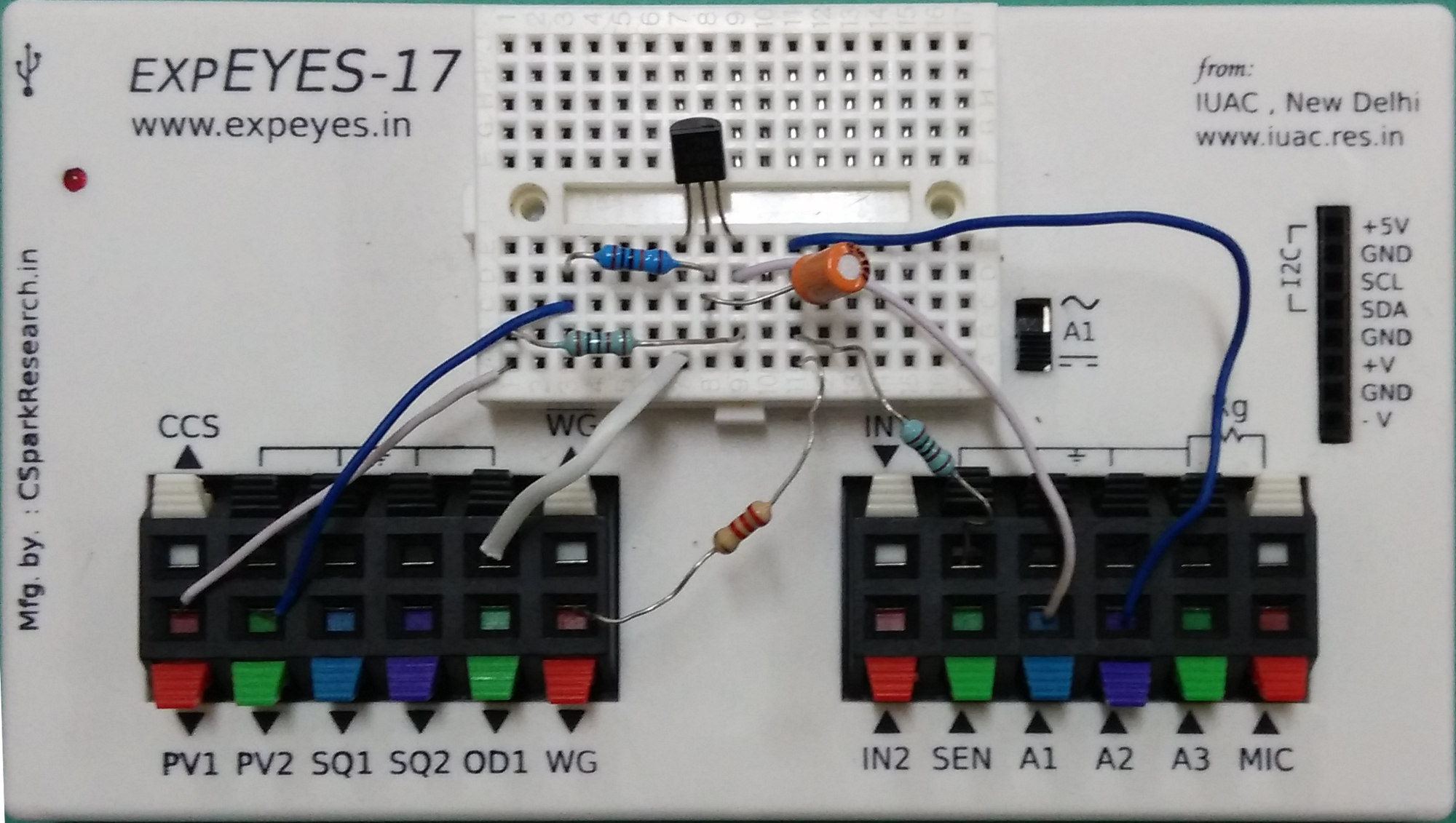
The schematic is wired as shown in the diagram below. It is very similar
to the schematic used for drawing the output characteristics. The AC
signal is connected to the base, through a capacitor so that the biasing
is not affected. Since the gain is high, we need a small input signal,
smaller than the 80 mV available from WG. A divider network using 1k and
2.2k gives around 20 mV output and that is fed to the base. This input
signal is monitored on A2. The DC operating point is decided by the
voltage applied to the base through the 100k resistor. By adjusting PV2,
we can take the transistor between cut-off and saturation conditions.
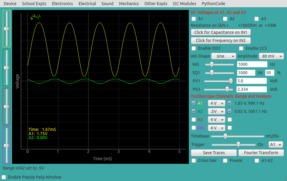
The value of PV2 is adjusted to get an output with minimum distortion.
To improve it further, one can reduce the input signal, use a higher
collector supply voltage instead of PV1, or use a transistor with a
lower gain value.
Wiring Diagram
Photograph of the experimental
setup. Transistor is 2N2222
Screen shot of the input and output waveforms of Transistor Amplifier
in CE configuration